|
 |
||||||||||
 |
|||||||||||
| Accueil > Artois teams > Thin Films & Nanomaterials > Thin films and electrical properties at the nanoscale | |||||||||||
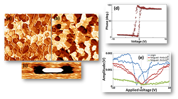
Thin Films & Nanomaterials:Thin films and electrical properties at the nanoscale:Studies that underlie the understanding of the physical properties of matter at nanometer scales bear fundamental significance in the context of permanently increasing miniaturization of electronic devices. With this respect, the atomic force microscopy (AFM) proves to be a prime tool in the characterization of such nano-materials. In this context, the investigations led within our team are devoted to the characterization of piezo-/ferroelectric properties of oxide thin films along with their integration into nano-devices (ferroelectric memories, micro/nano-electromechanical systems... ). The piezo-response mode (PFM) of the AFM, both in imaging and spectroscopic modes (piezoloops), is specifically developed and used to study the electromechanical activity (evaluation of the piezoelectric coefficient), the architecture of ferroelectric domains (Fig. 1a-b), the behavior of domain switching (coercive voltage; Fig 1c -d) , the electrical fatigue ( Fig. 1e; [P1]) and the effect of imprint (self-polarization, pinning, [P2])in piezo-/ferroelectric oxides thin films such as PbZrxTi1-xO3 (PZT), Pb1-3y/2LayZrxTi1-xO3 (PLZT), Pb(Mg1/3Nb2/3)O3-PbTiO3 (PMN-PT), ) and, more recently, Ln2Ti2O7 (Ln = Lanthanide),as well as in films multiferroic BiFeO3 (BFO) or (BiFeO3)m/(SrTiO3)n superlattices [P3].
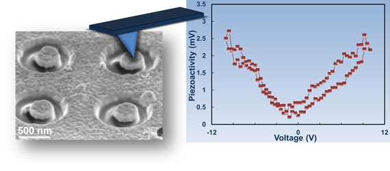
In addition, special attention is given to the following issues: i)the influence of the nature of the substrate and/or the bottom electrode, ii)the deposition conditions, iii)the thickness of the deposited film [P2], iv)the preferred crystallographic orientation [P4] and v)the special treatment applied to the film (etching, [P5]) ]). Furthermore, nanostructured thin films obtained with Ga+focused ion-beams (FIB) are considered in order to evaluate both the influence of etching and other potential size effects that are initiated following material-removal on the physical properties of fabricated piezo-/ferroelectric nano-objects (nano-islands) (Fig. 2; [P6, P7]).
Parts of these works are carried-out in collaboration with external laboratories (CRISMAT Laboratory in Caen, IEMN in Lille1 ...). On the experimental side, several works have been simultaneously carried-out with modeling studies that directly relate the ab-initio study of the structural, electronic, and ferroelectric properties of thin films, using quantum-chemistry methods. It is worth-mentioning that during the last few years, our team has led the majority of its work on the study of new environmentally acceptable films, on the basis of an internal collaboration with the "innovative and oxides derived phases" team of the UCCS and mainly relates to the development of new phases in bulk and their development in thin films.
Publications :
|
|||||||||||
 |
|||||||||||
 |
| |
|
|
|
|
| |
|
|
|
| |